BareMetal Logic Documentation
Overview
BareMetal Logic is a sandbox pixel-based digital logic simulator that is designed to be as true-to-life as possible whilst circumventing the oddities of real semiconductor development. The project has the major goal of being highly performant on modest hardware such that it can be used to simulate large-scale circuits such as the Intel 8080 CPU.
Features
- Pixel-based wire drawing + erase tools
- Live 3D voxel view of the multi-layer circuit
- Real-time simulation with speed (TPS) controls
- Minimap (manual refresh or live updates)
- Copy / cut / paste with a live “ghost” preview
- Multi-layer editing for complex circuits
- Branching history timeline with jump-to-node, undo/redo, play/rewind controls, and dead-branch visualization
- Major performance improvements for huge TPS runtime speeds
Game Logic Rules
The simulation follows six core rules that govern circuit behavior:
| Rule | Category | Description |
|---|---|---|
| 1a | Wire Formation | Pixels create wires. Adjacent non-transparent pixels are grouped together to form conductive wires. |
| 1b | Wire Types | Two wire types exist: (1) Shielded wires (red/orange color scheme) do not interact between layers and require explicit vias; (2) Unshielded wires (pink color scheme) allow 3D charge transfer between vertically aligned pixels on adjacent layers. |
| 1c | Power Levels | Seven discrete charge levels (0-6) are represented by pixel brightness. Each wire type has its own color palette: Shielded uses dark red (charge 0) through yellow-orange (charge 6); Unshielded uses dark pink through light pink. |
| 1d | Layer Transfer | Cross-layer charge transfer incurs a power loss. When unshielded wires transfer electricity between layers, there is effectively a 1-charge drop in the propagation. |
| 2 | Wire Crossings | Plus (+) configuration creates wire crossings. Four wires meeting at a pixel (top, bottom, left, right) with no diagonal connections form independent vertical and horizontal charge paths. |
| 3a | Transistor Formation | T-shaped configuration creates transistors. Three wires meeting at an empty pixel (with specific missing diagonal neighbors) form a switching element. The base controls charge flow between two terminals. |
| 3b | Transistor Delay | Transistors introduce propagation delay. Charge passes through with 1-tick delay. When the gate/base is unpowered, charge flows through with a 1-level drop. |
| 3c | Transistor Formula | Output charge calculation: output = input - 1 - gateCharge. When
gate charge is 0, output is 1 less than input. Higher gate charge further reduces output,
effectively blocking the signal when gate charge is high enough. |
| 4 | Power Sources | 2x2 pixel blocks create power sources. When four pixels form a square, the resulting wire becomes an infinite charge source, continuously supplying the maximum power level. |
| 5 | Layer Propagation | Higher layers have lower propagation delay. This allows designers to route paths on upper layers for faster signal propagation. |
| 6 | Wire Length Effects | Longer wires take longer to charge up through transistors. This delay behavior means you need to design synchronous components like latches and flip-flops carefully to ensure stable clock distribution and avoid race conditions in multi-stage logic. |
Architectural Details
Simulation Engine Core
The simulation engine is built around an event-driven work queue model that improves performance over scanning every wire. This approach only processes wires that might change, leading to speedups on circuits where only a small fraction of wires are active at any given time.
Initial Wire Grouping (Constructor)
The Simulation constructor performs three passes to construct the circuit topology from a palette image. The first pass groups pixels into wires using a bucket-fill algorithm in O(N) time. It converts the palette index to a charge level and checks the top and left neighbors to merge them using a union-find approach. This detects power sources when a 2x2 block is formed.
// First pass: group pixels into wires using bucket-fill
for (int y = 0; y < sizeY; y++) {
    for (int x = 0; x < sizeX; x++) {
        uint8_t paletteIndex = img.pixels[y * sizeX + x];
        if (paletteIndex == 0) continue; // transparent/black - skip
        uint8_t charge = paletteIndex - 1; // convert palette index to charge

        Bucket* topBucket = matrix.get(x, y - 1);
        Bucket* leftBucket = matrix.get(x - 1, y);

        // If neighbors belong to different groups, merge them
        if (topBucket != nullptr && leftBucket != nullptr && topBucket->group != leftBucket->group) {
            Group* groupToMerge = topBucket->group;
            groups.erase(groupToMerge);
            groupToMerge->moveContentTo(leftBucket->group);
            delete groupToMerge->wire;
            delete groupToMerge;
        }

        // Detect power sources: top-left diagonal indicates 2x2 block
        if (topLeftBucket != nullptr && topBucket != nullptr && leftBucket != nullptr) {
            currentBucket->group->wire->setIsPowerSource(true);
        }
The second pass handles crossings in plus (+) patterns by checking for a plus pattern and merging vertical
and horizontal groups. The third pass detects transistors in T patterns, where each T orientation creates a
transistor with
base, inputA, and inputB. Sometimes, transistors are detected as wire
crossing, this is a non-issue as the first stage properly
identifies all transistors.
Event-Driven Simulation Step
The simulation operates in two distinct phases:
- Phase 1 performs read-only computation, iterating only over the active work queue (not all wires). For
each active wire, it computes the next charge based on the current global state snapshot. Power sources
ramp up by +1 per tick until reaching
MAX_CHARGE(6). Normal wires usetracePowerSourceCharge()to find the strongest available charge from connected sources. The relaxation dynamics ensure wire charge can only change by ±1 per tick: if the source is stronger, charge increases by 1 (charging up); if the source is weaker or equal and the wire has charge, it discharges by 1 (draining). This prevents instant propagation and creates realistic RC-like delay behavior. All computed next values are stored inpendingCharges[]without modifying thecharges[]array yet. - Phase 2 applies all pending changes pixel-by-pixel, which is now safe since all computations have finished. For each wire that actually changed, the system re-enqueues it (as it might need more ticks to reach equilibrium), wakes value neighbors (always, for wires connected through transistor terminals), and wakes gate neighbors conditionally (only on 0 ↔ 1 crossings).
The work queue lifecycle begins with all wires enqueued initially for circuit settling from a cold start. In
steady state, most wires settle and leave the queue. Activity bursts occur when toggling an input propagates
through the affected subcircuit only, while clock circuits and oscillators keep relevant wires perpetually
active. Considering this situation with the original implementation that scanned all wires every tick,
it ran
for (all wires) { recompute(); } achieving O(N) per tick, while the event-driven approach runs
for (active wires) { recompute(); } achieving O(changes) per tick.
size_t Simulation::step() {
    const int n = (int)charges.size();
    if (workQueue.empty()) {
        // Nothing currently active - circuit has settled
        return 0;
    }

    nextQueue.clear();
    lastChangedWires.clear();

    // Phase 1: Compute next charges (read-only snapshot)
    for (int idx : workQueue) {
        queued[idx] = 0; // allow re-queueing for next tick

        uint8_t charge = charges[idx];
        uint8_t next = charge;

        if (wireIsPowerSource[idx]) {
            // Power sources ramp up to MAX_CHARGE
            if (charge < MAX_CHARGE) {
                next = (uint8_t)(charge + 1);
            }
        } else {
            // Trace best available source charge
            uint8_t sourceCharge = tracePowerSourceCharge(idx);
            /* ... relaxation dynamics ... */
            if (sourceCharge > (uint8_t)(charge + 1)) {
                next = (uint8_t)(charge + 1);
            } else if (sourceCharge <= charge && charge > 0) {
                next = (uint8_t)(charge - 1);
            }
        }

        if (next != charge) {
            pendingCharges[idx] = next;
            lastChangedWires.push_back(idx);
        }
    }

    // Phase 2: Apply changes and propagate events
    for (int idx : lastChangedWires) {
        uint8_t next = pendingCharges[idx];
        uint8_t prev = charges[idx];
        charges[idx] = next;
        ++changeCount;

        // Enqueue this wire for continued settling
        enqueueWire(idx, nextQueue, queued);

        // Wake up neighbors affected by this change
        const bool gateCriticalCross = ((prev == 0) != (next == 0));

        // ... wake value neighbors and gate neighbors ...
        if (gateCriticalCross) {
            /* ... wake gate neighbors ... */
        }
    }

    workQueue.swap(nextQueue);
    return changeCount;
}
Flattened Power Source Tracing
Previously, the system used pointer-chasing through Wire* → Transistor* →
Wire*, which was cache-unfriendly. The new implementation uses Compressed Sparse Row (CSR) adjacency lists.
The build process creates SrcEdge structures for each wire, storing pairs of
(other_wire,
blocking_base). These are then flattened into CSR arrays where sourcePtr[wire_id]
gives the start index.
All data for a wire's edges is stored contiguously in memory.
The memory layout becomes highly cache-friendly, providing sequential reads where the prefetcher
loads entire cache lines ahead of time. The trace function becomes a linear loop over the
sourcePtr arrays,
iterating through edges to check if the transistor gate is blocking and sample the charge from the connected
wire.
void Simulation::buildAdjacency() {
    // Build CSR-format source adjacency: for each wire, store (other_wire, blocking_base)
    /* ... build adjacency logic ... */

    // Flatten into CSR arrays (cache-friendly linear scan)
    for (int i = 0; i < n; ++i) {
        sourcePtr[i + 1] = sourcePtr[i] + (int)src[i].size();
        sourceTotal += src[i].size();
    }
    /* ... flatten loops ... */
}
Multi-Layer Cross-Coupling
For unshielded wires, the system implements event-driven cross-layer coupling. A pixel-level approach would scan each pixel (x, y) in layer A, check if it is unshielded and whether layer B has an unshielded pixel at (x, y), then directly copy charge. This is O(width x height) work per tick and prevents event-driven optimization.
The wire-level solution operates in two phases. At build-time, the system maps pixels to wire indices and creates bidirectional edges between coupled wires. At run-time, for each wire that changed in layer A, it iterates coupled wires in layer B, recomputes the external source charge, and marks the wire dirty if needed.
The external source charge mechanism treats cross-layer coupling as another power source. Each simulation
maintains externalSourceCharge[wire_index], and during tracePowerSourceCharge()
the system computes max(internal_sources, externalSourceCharge). This scales well as coupling
work is proportional to active wires.
static void rebuildUnshieldedCouplingAdjacency(AppState& state) {
    // Build wire-to-wire coupling edges between adjacent layers
    for (int a = 0; a < layerCount; ++a) {
        // ... iterate only over cached unshielded pixels (sparse set) ...
        const auto& pixels = state.unshieldedPixelIndexLayers[a];
        std::vector pairs;
        for (int p : pixels) {
             /* ... map pixels to wires and create edges ... */
        }
        /* ... deduplicate and build bidirectional edges ... */
    }
}
Batched Rebuild Optimization
During interactive drawing (e.g., right-click drag to erase), calling rebuildLayerSimulation()
per pixel caused freezes on large canvases because rebuilds are O(N) operations.
The old behavior (per-pixel rebuild) was slow when the user drags mouse to erase a large number of pixels in
a
stroke. The new behavior (batched rebuild) is better where the user drags mouse to erase
many pixels in a stroke, then during this stage set each pixel to 0. On mouse
button release just run rebuildLayerSimulation()() once, reducing the number of rebuilds and
freezes.
The implementation tracks gesture state when the erase gesture starts (eraseDragActive
becomes true), it records the layer and clears the dirty flag. During drag, pixels are modified directly in
the
image with no rebuild. The user sees immediate visual feedback through direct pixel manipulation. After
rebuild on gesture end, the simulation takes over with the new topology.
// On mouse button release
if (state.eraseDragActive) {
    state.eraseDragActive = false;
    if (state.eraseDragDirty) {
        rebuildLayerSimulation(state, state.eraseDragLayer); // Rebuild once
        state.eraseDragDirty = false;
    }
}
3D Graphics System
The 3D voxel viewer provides real-time visualization of multi-layer circuits as stacked volumetric structures, implemented entirely on the CPU without GPU dependencies.
Voxel Cache Building
The system pre-builds a cache of voxel instances with rotated coordinates to map 2D stacked layers into 3D space. The 2D canvas layout represents layers with X as horizontal on the canvas, Y as vertical on the canvas, and layers stacked conceptually behind each other. In 3D voxel space, this maps to Z as height (from the original Y axis), X as depth (negative original X axis), and Y as layers (negative layer index).
Voxel instance creation is sparse and efficient. Each non-transparent pixel becomes one voxel. Color is directly copied from the palette, showing current charge via hue. WireType is stored per-voxel for material and color determination later. The sparse representation only stores occupied voxels, not 1M empty cubes for a 1000x1000x4 volume.
static void rebuildVoxelCache(AppState& state) {
    state.voxelView.voxelInstances.clear();
    for (int layer = 0; layer < (int)state.simulationImages.size(); ++layer) {
        /* ... iterate pixels ... */
        // Rotate coordinate frame: x → -z, layer → -y, y → z
        v.x = (-1) * x;
        v.y = (-1) * layer;
        v.z = y;
        state.voxelView.voxelInstances.push_back(v);
    }
}
Software Rasterizer
A lightweight CPU-based triangle rasterizer renders voxels as shaded cubes using barycentric coordinate interpolation with depth testing. I prioritized simplicity and portability over raw performance (like using OpenGL).
The algorithm proceeds in five steps:
- Bounding box computation: finds min/max X/Y of triangle vertices, testing only pixels in this rectangle for early rejection of off-screen triangles.
- Barycentric coordinate computation: for each pixel in the bounding box, compute weights
w0,w1,w2that determine if the pixel is inside the triangle. - Inside test: if all weights are non-negative, the pixel is inside the triangle.
- Depth interpolation: computes
depthusing $\text{depth} = w_0 z_0 + w_1 z_1 + w_2 z_2$, which provides smooth interpolation across the triangle face. - Depth test: only update the pixel if the new depth is closer than the existing depth, handling back-to-front occlusion.
Barycentric
coordinates represent how much each vertex contributes to a pixel's
position. The weights w0, w1, w2 form a coordinate system where $w_0
+ w_1 + w_2 = 1$ inside the triangle. If a pixel is closer to vertex 0, its depth approaches
z0, and similarly for other vertices. The pixel center is sampled at
(x + 0.5, y + 0.5) for proper anti-aliasing behavior.
The depth buffer maintains a Z-value per pixel. When a triangle is rasterized, each pixel's depth is interpolated from the three vertex depths using barycentric weights. If the new depth is less than the stored depth (closer to camera), both the depth buffer and the color buffer are updated. This provides correct occlusion without needing to sort triangles.
void rasterizeTriangle(const Vertex& v0, const Vertex& v1, const Vertex& v2, Buffer& buf) {
    // 1. Bounding box
    int minX = std::max(0, std::min({v0.x, v1.x, v2.x}));
    int maxX = std::min(buf.width - 1, std::max({v0.x, v1.x, v2.x}));
    int minY = std::max(0, std::min({v0.y, v1.y, v2.y}));
    int maxY = std::min(buf.height - 1, std::max({v0.y, v1.y, v2.y}));

    // Precompute denominator (2x triangle area)
    float denom = (v1.y - v2.y) * (v0.x - v2.x) + (v2.x - v1.x) * (v0.y - v2.y);
    if (std::abs(denom) < 1e-5) return; // Skip degenerate triangles

    for (int y = minY; y <= maxY; y++) {
        for (int x = minX; x <= maxX; x++) {
            // 2. Barycentric coordinates
            float w0 = ((v1.y - v2.y) * (x - v2.x) + (v2.x - v1.x) * (y - v2.y)) / denom;
            float w1 = ((v2.y - v0.y) * (x - v2.x) + (v0.x - v2.x) * (y - v2.y)) / denom;
            float w2 = 1.0f - w0 - w1;

            // 3. Inside test
            if (w0 >= 0 && w1 >= 0 && w2 >= 0) {
                // 4. Depth interpolation
                float z = w0 * v0.z + w1 * v1.z + w2 * v2.z;

                // 5. Depth test
                if (z < buf.depth[y * buf.width + x]) {
                    buf.depth[y * buf.width + x] = z;
                    buf.pixels[y * buf.width + x] = shadePixel(v0, v1, v2, w0, w1, w2);
                }
            }
        }
    }
}
Lighting Model
Multi-light shading with backface culling provides visual depth. I use three orthogonal lights because a single light creates harsh shadows. The main light mimics a "sun" position, and two orthogonal lights ensure no face is ever completely dark.
Per-face lighting computation starts by checking the face normal n against the view vector for
backface culling.
For visible faces, the system computes ndotl using Lambert's cosine law.
After accumulation, an ambient term is added to prevent pure black faces.
Wire color encodes charge (game state) while shade encodes geometry (depth).
// Lambert's cosine law
float ndotl = std::max(0.0f, v3_dot(n, v3_scale(lightDirs[li], -1.0f)));
shade += ndotl * 0.5f;

// Apply lighting to wire color (color from charges, brightness from lighting)
Color wireCol = getWireColor(v.wireType, v.charge);
uint8_t rC = (uint8_t)clampv(int(wireCol.r * shade), 0, 255);
Camera System
The camera system supports both perspective and orthographic projection with orbit, pan, and zoom controls.
Spherical coordinates provide an orbit camera where yaw is horizontal rotation,
Pitch is vertical rotation,
and Distance is the zoom level.
An orthonormal camera basis transforms world coordinates to camera space. Perspective projection divides by depth to create the converging-lines effect, while Orthographic projection uses fixed scale with no depth division, useful for technical drawings.
Future Work
- Bus tool for easier bus-line routing, and other blueprinting tools
- A chip-blueprint library and chip-optimization routine for uber-fast circuits
- Import Verilog and convert into circuits
- Assembly editor + assembly memory support
- Time-control / signal playback dock for propagation debugging
- Wire probing + waveform/clock-diagram view
- More realistic wire behavior options (delay/charge/current flow) + metastability visualization (readable, colored wires)
- Pixel palette for backgrounds and labels as separate color
- Multi-colored wires (shared lightening formula)
- SIMD vectorization for increased performance
- Multithreaded layer stepping where you can run independent layers in parallel.
- JIT compilation where you compile stable subcircuits into native loops.
- Use a GPU for the rasterizer using Vulkan or OpenGL.
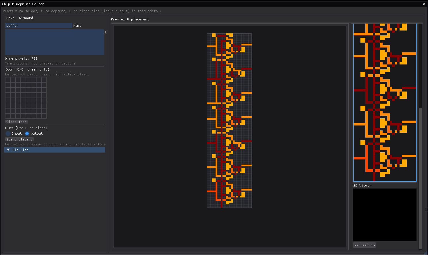
Above is the chip blueprint editor which is still a work-in-progress. Plans include to allow for chips to be treated as blackboxes such that only their truth-table and propagation delay is preserved. This further reduces simulation times as the truth-table can be precalculated.